Current generated glides via clips positioned on the earlobes Output present adjustable from eighty to 600 microAmperes
Owing to the recent launching in Europe of Cranial Electrotherapy Stimulation (CES) transportable sets, we have been "Electronically Stimulated" in designing a identical circuit for the sake of hobbyists. CES is the most popular method for electrically boosting mind energy, and has long been prescribed by way of physicians, majorly in the USA, for therapeutic purposes, together with the therapy of hysteria, depression, insomnia, and chemical dependency. CES gadgets generate an adjustable present (80 to 600 microAmperes) that go with the flows through clips positioned on the earlobes.
The waveform of this software is a four hundred milliseconds optimistic pulse followed by using a negative probably the most related duration, then a pause of 1.2 2ds. The major frequency is 0.5 Hz, i.e. a double pulse every 2 2ds. Some people file that this type of minute specialized electrical impulses make contributionss to achieve a calm state that departs the thoughts alert. Obviously we cant declare or prove any therapeutic effectiveness for this device, but if you're considering trying it, the circuit is so low-cost and so simple to build that an try might be made with somewhat no hurt.
Circuit diagram:

R1___________1M5 1/4W Resistor
R2___________15K 1/4W Resistor
R3___________100K Linear Potentiometer
R4___________2K2 1/4W Resistor
C1___________330nF 63V Polyester Capacitor
C2___________100µF 25V Electrolytic Capacitor
D1___________3mm. Red LED
IC1___________7555 or TS555CN CMos Timer IC
IC2___________4017 Decade relyer with 10 decoded outputs IC
SW1__________SPST Slider Switch
B1____________9V PP3 Battery Clip for PP3 Battery
Two Earclips with wires (see notes)
Circuit operation:
IC1 forms a narrow pulse, 2.5Hz oscillator feeding IC2. This chip generates the quite quite a bit of timings for the output pulses. Output is taken at pins 2 & three to simply receive poor going pulses also. Current output is professionalscribed to 600µA via R2 and shall be regulated from 80 to 600µA by means of R3. The LED flashes every 2 2ds signaling right form operation and will additionally be used for setting functions. It will likely be unnoticed together with R4, very much rising battery life.
- In order to acquire a more actual frequency setting take R1=1M2 and add a 500K trimmer in series with it.
- In this case use a frequency meter to learn 2.5Hz at pin three of IC1, or an oscilloscope to read 400msec pulses at pins 2, three or 10, adjusting the brought trimmer.
- A simpler environment might be made adjusting the trimmer to depend precisely a LED flash each 2 2ds.
- Earclips will probably be made with little plastic clips and cementing the tip of the wire able appropriate to make good contact with earlobes.
- Ultra-simple earclips will doubtless be made the use of a thin copper foil with rounded corners four cm. lengthy and 1.5 cm. extensive, soldering the wire finish within the middle, and then folding the foil in two phases holding the earlobes.
- To make certain a better present transfer, this sort of devices on an ordinary basis has felt pads moistened with a conducting resolution interposed between clips and pores and skin.
- Commercial sets have frequently a built-in timer. Timing sessions remaining usually 20 minutes to 1 hour. For this goal you must utilize the Timed Beeper the Bedside Lamp Timer or the Jogging Timer circuits to be had on this site, adjusting the timing parts so as to fit your wants.
Source:www.ecircuitslab


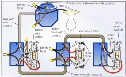
 230Vac Lamp Toggle Switch Circuit diagram


 However, before you may need to think of the basic home theater design for your home theater system, you may need to know the size of the room for the home theater set up. The size of the room to where the home theater will be set up will depend on how basic the home theater design needs to be.